Bend Radius for a Flexible Printed Circuit
When designing a flexible printed circuit, you must specify the bend radius for your design. It is the minimum degree that a flex PCB can bend before it begins to experience permanent damage, and this is vitally important for the success of any flex circuit application. The bending of a flexible printed circuit board can cause stress on the copper conductors, which can cause them to degrade and fail. This damage can be caused by a variety of factors, including improper bending and the use of an inadequate bend radius.
Specifying the correct bend radius will prevent your flex circuit from suffering from damage, and will help to ensure that it can operate properly in any environment. To do this, you must first understand how a flex PCB is manufactured. This will allow you to choose the right materials for your flex PCB and calculate the appropriate bend radius.
A flexible printed circuit is made up of several layers, which include the insulator, metal foils and conductors. The conductors are etched from the metal foil and are usually composed of copper, though other types can be used as well. The insulator is used to separate the electrical conductors from each other and is often made from materials such as polyimide, solder mask or polyethylene naphthalene. The conductors are then soldered to the insulator using either an epoxy or acrylic adhesive.
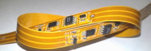
Specifying the Bend Radius for a Flexible Printed Circuit
The thickness of a flex circuit board is a factor in its flexibility. Thicker boards are less flexible, while thinner ones offer more flexibility. Regardless of thickness, the bend radius must be determined early in the design process. In addition to identifying the optimum thickness of a flex PCB, you must also determine whether it will be used in a dynamic or stable flex configuration. If the flex circuit will only be bent once, such as in the case of a flex to install design, then the minimum bend capability can be as low as six times the finished flex thickness.
If the flex circuit is going to be subjected to repeated bending over its lifetime, the bending capabilities must be much higher. This requires a different approach to the design of the flex circuit. To improve the durability of a dynamic flex PCB, it is advisable to stagger traces on all layers and to avoid I-beaming. This will minimize stress concentrations in the copper and enhance flexibility and reliability.
In addition, the traces should be narrower in the flexible sections of the circuit. This will further reduce stress concentrations and the likelihood of tearing. It is also advisable to place thicker dummy traces around the flexible areas of the circuit as an added safeguard against tearing. These dummy traces do not have any electrical function, but serve to protect the traces from excessive strain. Lastly, all vias and slits in the flexible section of the circuit should be designed-in relief holes. These will reduce the stresses that can be created by bending and will increase the lifespan of the flex circuit.